
Summary
Semiconductor manufacturing facilities face stringent cleaning requirements that directly influence product performance, yield rates, and operational costs. Conventional cleaning approaches frequently involve manual hand cleaning, harsh chemicals, extended downtime, and hazardous waste streams. Dry ice cleaning is non-abrasive and non-conductive, produces no secondary waste, and enables equipment decontamination without disassembly, delivering ultra-precise contaminant removal throughout the semiconductor value chain.
What is dry ice blasting used for in semiconductor and PCB manufacturing?
Dry ice blasting is a non-abrasive, dry cleaning method used across the semiconductor and PCB value chain—polysilicon production, wafer fabrication, semiconductor assembly, and PCB manufacturing. Solid CO₂ sublimates to gas on impact, removing particles, oils, photoresist, polishing compounds, flux, and conformal coatings without chemicals, moisture, or secondary waste. It cleans CVD reactors, wafer chambers, deposition tooling, molds, dies, PCBs, and ICT fixtures in-place—often without disassembly or cool-down. Because it is non-abrasive, it won't alter the precise dimensions or surface finishes of wafers and tooling, and because it is a completely dry process, it safely cleans electrical harnesses, connectors, and boards without water damage or short-circuiting. The result is ultra-clean, contamination-free components that improve yield and reduce scrap. Cold Jet has more than 24,000 machines installed globally, from handheld units to automated robotic systems.
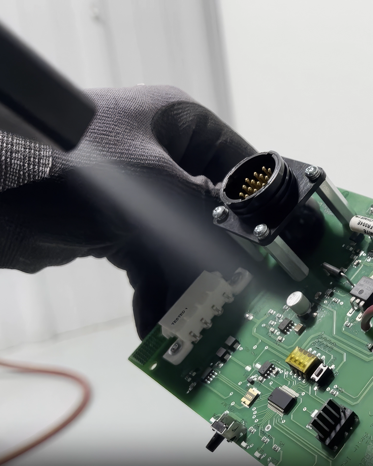
Conventional Cleaning Risks Yield and Purity
Conventional semiconductor cleaning approaches frequently involve manual hand cleaning, harsh chemicals, extended downtime, potential substrate damage, and hazardous waste streams. High-pressure water blasting and manual chemical scrubbing used to decontaminate CVD reactors are inefficient and time-consuming, expose workers to hazardous chemicals, can damage valuable equipment, and create secondary waste streams that require costly disposal, limitations that lead to production downtime and can compromise the purity and yield of the final product.
Higher Yield
Fewer Contamination Defects
Solvent-Free
No Chemical Cleaning
Cleanroom-Ready
Dry, Non-Conductive Process
Automation-Ready
Robotic Integration Available
Benefits of Dry Ice Cleaning in Semiconductor Manufacturing
Dry ice blasting delivers superior cleaning results for the semiconductor manufacturing chain by improving process efficiency, enhancing product quality, and extending equipment lifespan.
Dry ice blasting consistently improves production efficiency across semiconductor operations. Whether cleaning CVD reactors, decontaminating deposition tooling, cleaning semiconductor parts, or cleaning semiconductor molding equipment, this method works faster and more effectively than traditional methods. It enhances component quality while reducing defects and rejected parts. Since dry ice sublimates instantly upon contact, it leaves no residue or secondary waste, ensuring ultra-clean semiconductor components.
 Efficiency
Enhanced Manufacturing Efficiency
Dry ice cleaning enables rapid in-place equipment cleaning and decontamination without disassembly or cool-down time. The semiconductor cleaning process removes contaminants instantly, allowing immediate processing resumption. Dry ice blasting in semiconductor manufacturing is frequently automated and integrated into existing production processes, significantly reducing downtime and boosting production.
 Precision Safe
Gentle on Wafers and Delicate Features
Dry ice cleaning is a non-abrasive and non-destructive cleaning process. The semiconductor parts cleaning process does not damage critical equipment and preserves the integrity of finished product specifications. Dry ice blasting does not alter the precise dimensions and intricate details of semiconductors, wafers, or tooling components. With dry ice blast cleaning, you can achieve a pure clean without affecting surface finishes or delicate features.
 No Residue
Contamination-Free Cleaning Results
Dry ice sublimates instantly when it hits a surface, generating no secondary waste. Zero chemical residues, moisture, or contaminants remain on components or equipment, preventing cross-contamination and ensuring high-quality components. This maintains the pristine conditions essential for subsequent processing steps.
 Defect prevention
Contaminant-Free Semiconductor Products
By thoroughly removing microscopic particles, oils, dust, fingerprints, and other residues, dry ice blasting helps to maintain the highest level of cleanliness, which is essential for preventing defects and ensuring the quality and functionality of the final semiconductor product.
What Can Dry Ice Blasting Clean in Semiconductor Manufacturing?
Dry ice blasting is a comprehensive cleaning solution for maintaining purity and efficiency at every stage of the semiconductor manufacturing value chain, from polysilicon and raw material production through wafer fabrication, semiconductor manufacturing and assembly, and PCB manufacturing and assembly.
- Polysilicon & Raw Material Production
- Wafer Fabrication
- Semiconductor Manufacturing & Assembly
- PCB Manufacturing & Assembly
Polysilicon & Raw Material Production
Polycrystalline silicon manufacturers face a critical challenge in preventing silicon buildup and dust inside their CVD reactors. Conventional cleaning relies on high-pressure water blasting and manual chemical scrubbing, which exposes workers to hazardous chemicals, risks damaging valuable equipment, and creates a secondary waste stream that requires costly disposal. These limitations extend downtime and can compromise the purity of the final product, affecting quality and yield. Dry ice blasting provides a safer, faster, and higher-purity alternative for decontaminating polysilicon production equipment.
CVD Reactor Decontamination
Dry ice blasting quickly removes silicon buildup and dust from CVD reactor interiors without damaging surfaces, preserving equipment integrity. The process eliminates harsh chemicals and solvents, improving worker safety and reducing environmental impact, and generates no secondary waste.
Purity and Yield Protection
Because dry ice sublimates on contact and introduces no moisture or chemical residue, the process prevents downstream contamination and significantly reduces impurities and scrap rates, protecting the quality of the final polysilicon product.
Wafer Fabrication
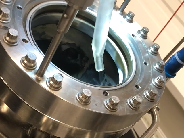
Dry ice blasting enables non-abrasive cleaning for the high-purity manufacturing of wafers.
Cleaning Wafer Chambers and Process Tooling
The delicate and complex nature of wafer fabrication equipment, including wafer chambers, deposition tooling, and polishing equipment, requires a cleaning method that is both highly effective and completely non-damaging. Dry ice blasting provides an ideal solution by dislodging contaminants without scratching or altering the precise surfaces of these critical components. The process allows for thorough cleaning of intricate parts, ensuring that tooling maintains its integrity and continues to perform optimally.
Decontaminating Plasma-Coated Fixtures and Surfaces
Following plasma coating processes for microchips or the use of polishing compounds on Teflon-coated aluminum chamber surfaces, a clean and residue-free environment is essential to prevent defects. Traditional cleaning methods can be overly aggressive or leave behind chemical residues that lead to cross-contamination. Dry ice blasting offers a superior alternative, as it is non-abrasive and leaves no secondary waste. This allows for the effective removal of stubborn build-up and polishing compounds from fixtures and chamber surfaces, ensuring the highest level of purity for subsequent production steps.
Maintaining Vacuum Pumps and Implanters
Vacuum pumps and implanters are vital to the wafer fabrication process, but they are also susceptible to contamination from process byproducts. The accumulation of these materials can degrade performance and lead to unplanned downtime. Dry ice blasting is a safe and efficient way to clean this specialized equipment. It can be performed in-place, eliminating the need for time-consuming disassembly and manual cleaning, while also being a completely dry process. This not only reduces maintenance time, but also protects these sensitive and expensive systems from damage associated with conventional cleaning techniques.
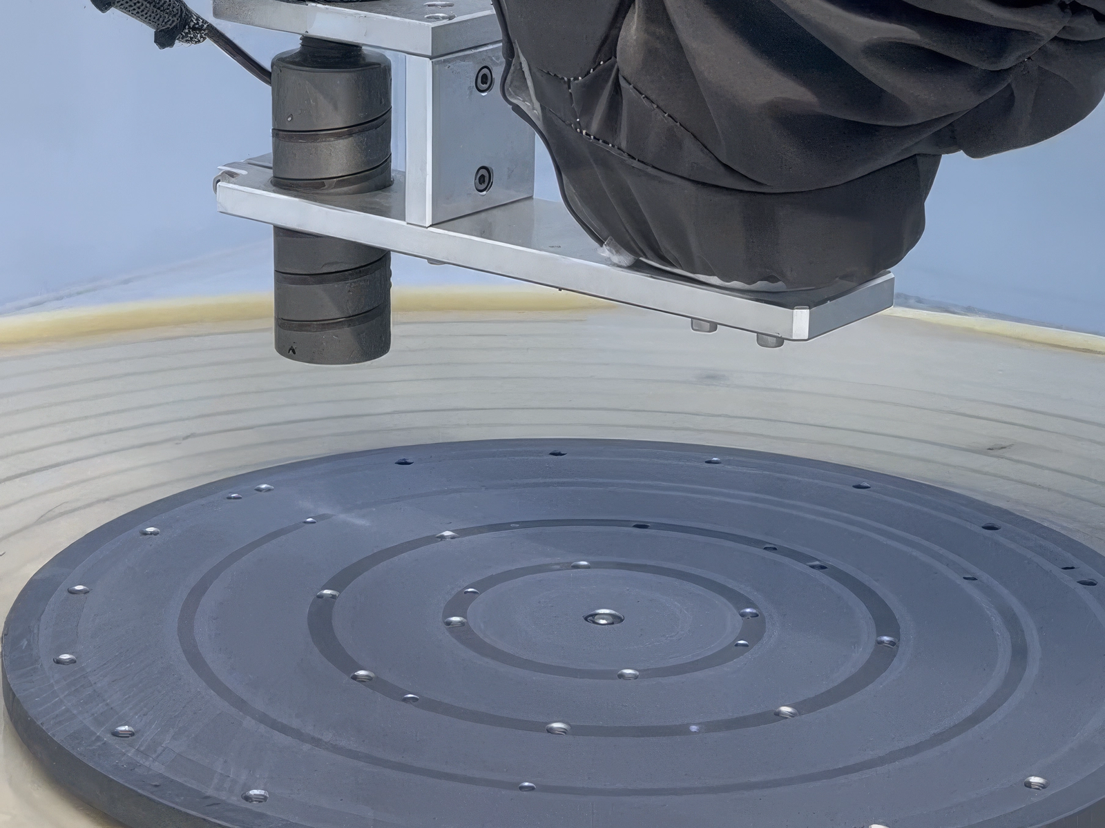
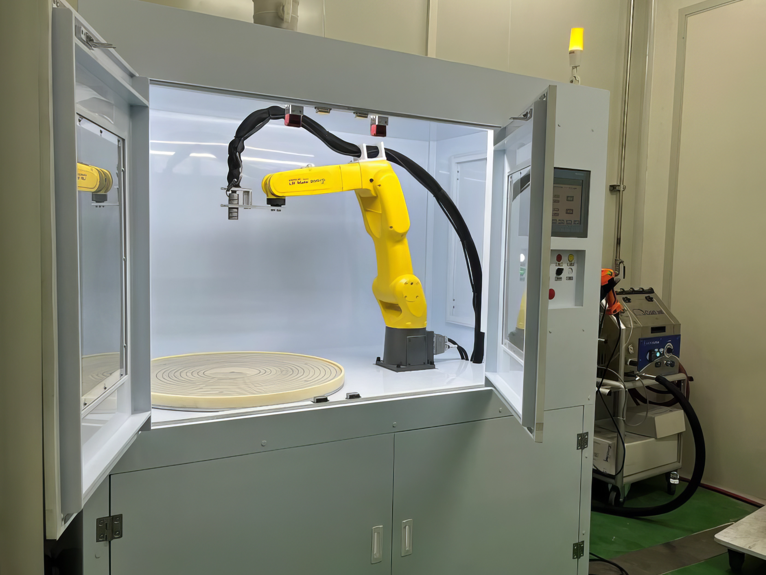
Semiconductor Manufacturing & Assembly
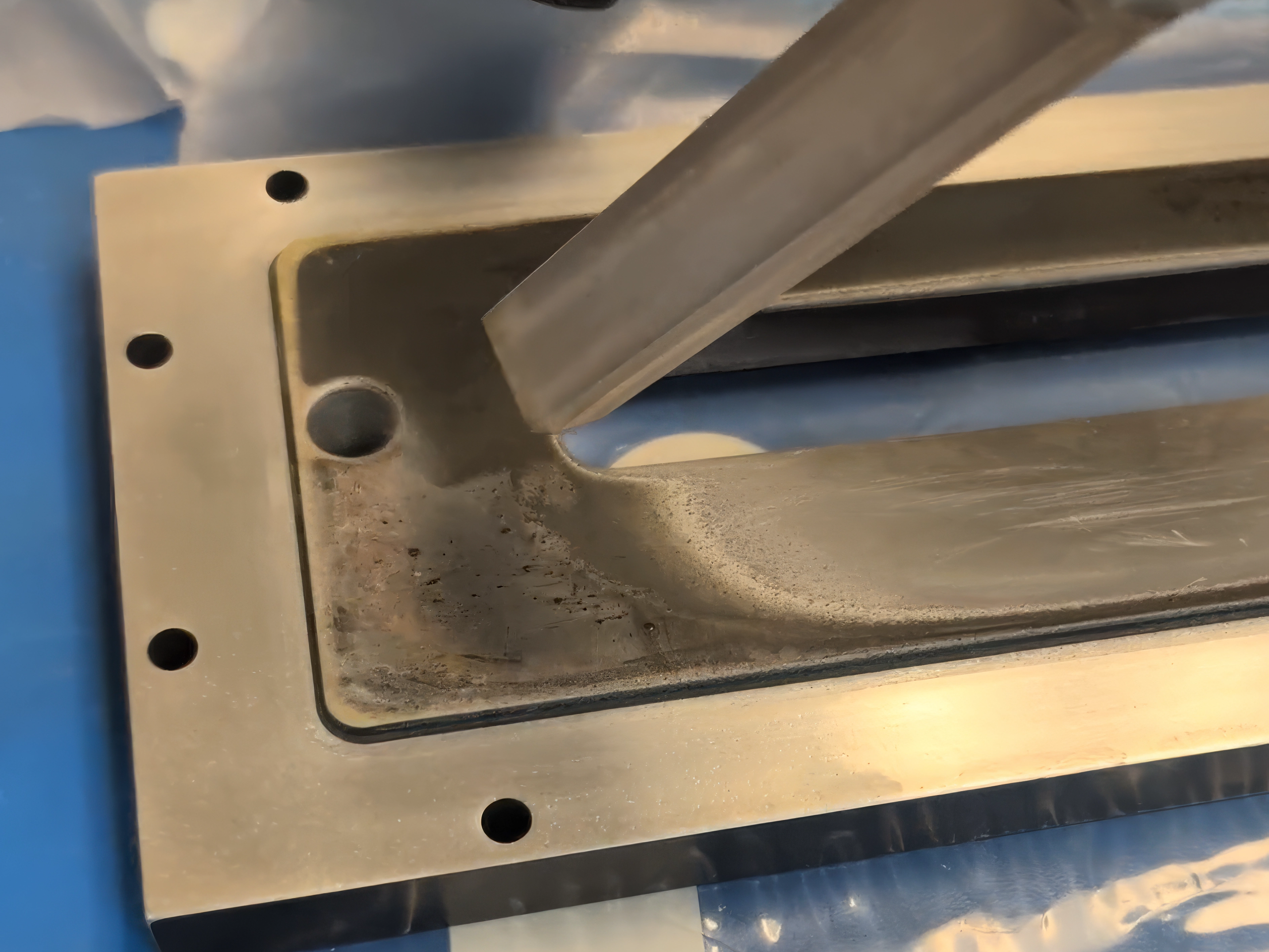
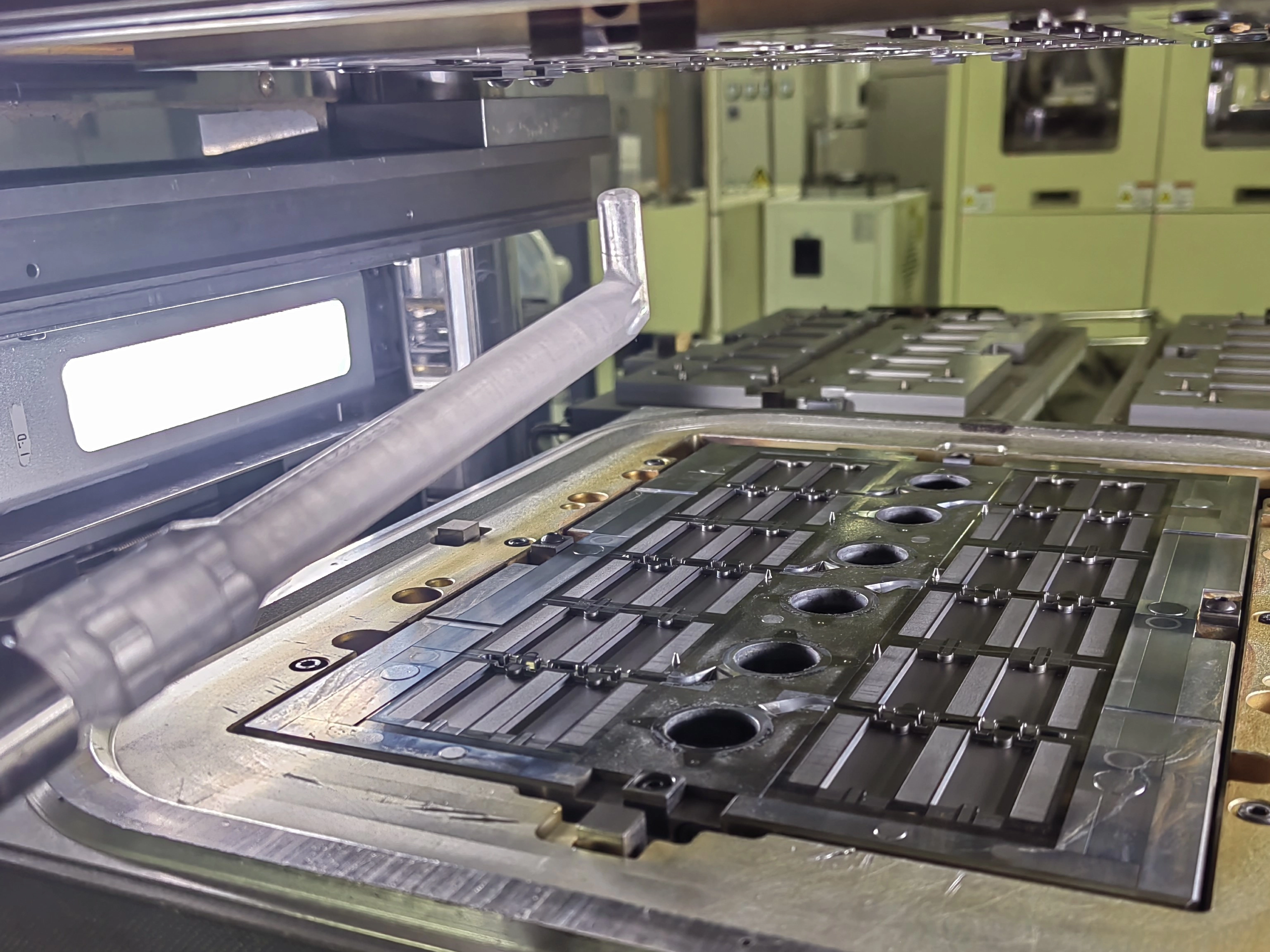
Dry ice blasting is a non-abrasive and residue-free semiconductor cleaning process.
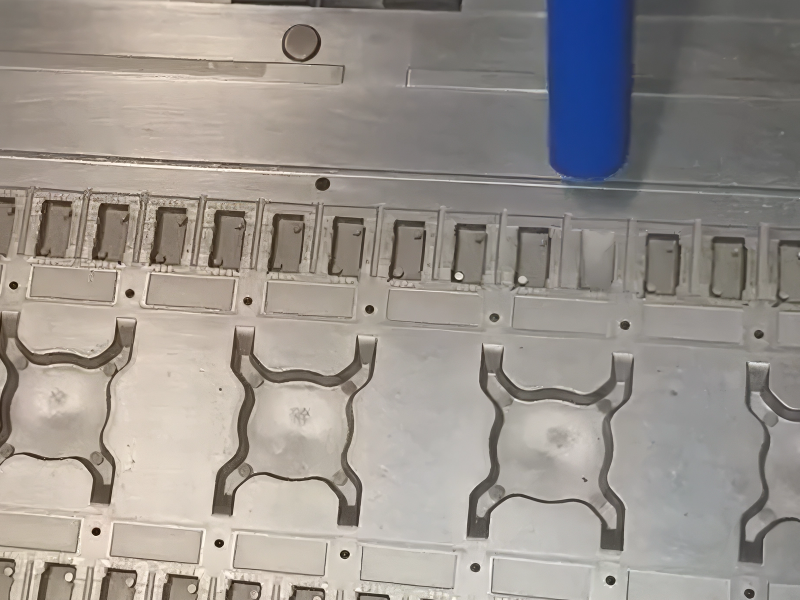
Molding & Die Cleaning
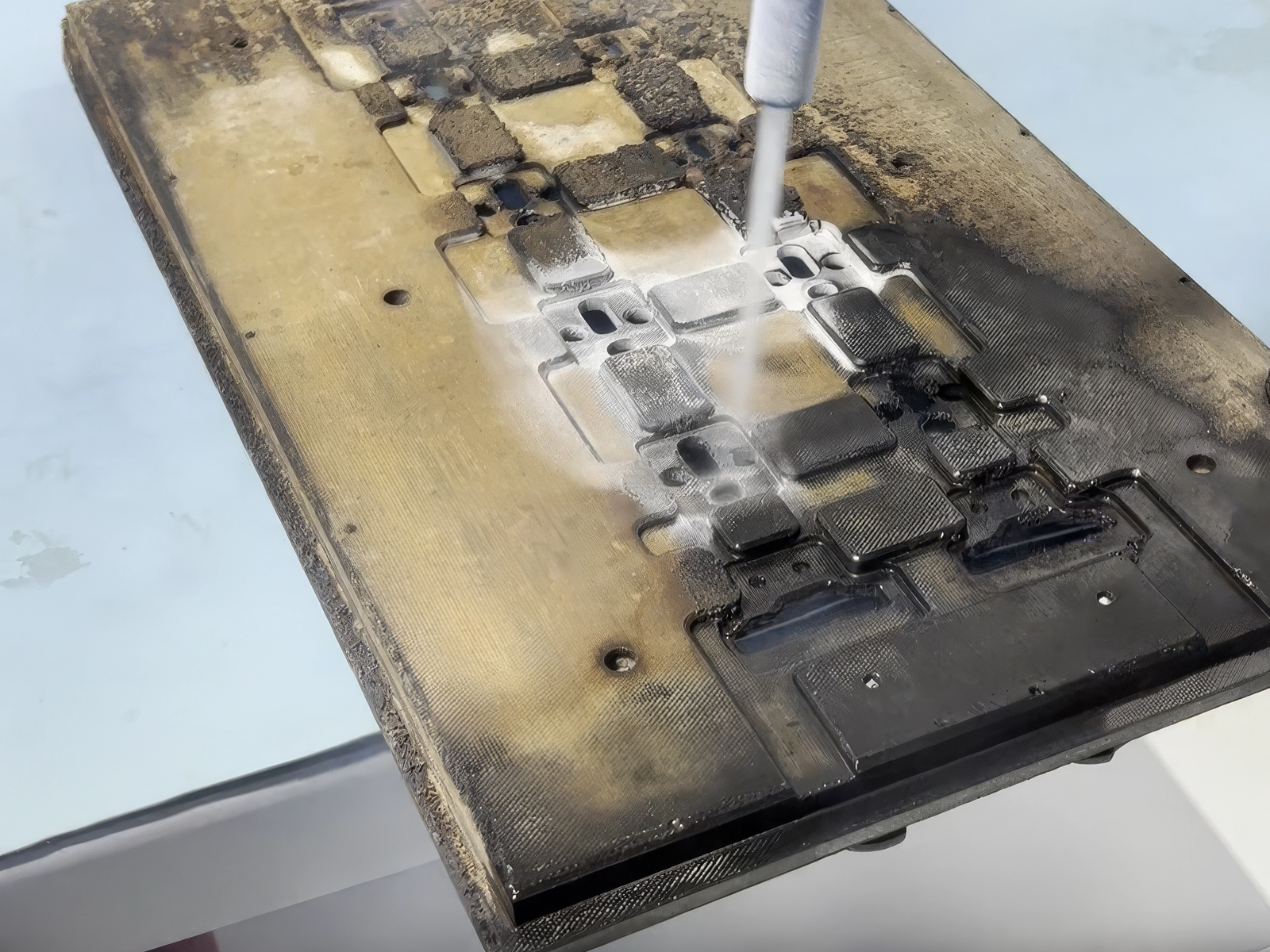
Contaminants like wax and gas buildup can foul the molds and dies used in semiconductor manufacturing, compromising the integrity of microchip carriers and molded components. Traditional cleaning methods are often time-consuming, requiring cool-down periods and manual scrubbing. Dry ice blasting is a superior alternative because it allows for in-place cleaning of molds and dies while they are still hot. This process effectively removes buildup without causing damage to the tooling, reducing downtime and maintaining consistent production quality.
Post-Processing Chip Finishing
After molding and laser-cutting, semiconductor parts can have unwanted debris like plastic flash or adhesives on their surfaces. These contaminants can affect performance or interfere with subsequent manufacturing steps. Dry ice blasting is an ideal semiconductor parts cleaning solution for post-process cleaning because it’s a non-abrasive method that removes debris without damaging the delicate chip edges or surfaces. This targeted cleaning process improves the quality of the finished product by ensuring a clean, precise component is ready for the next stage of manufacturing.
Component Cleaning & General Maintenance
Dry ice blasting is highly effective for general maintenance of a wide range of equipment and components. It’s a quick and efficient way to remove contaminants from machinery. The process is completely dry and non-conductive, allowing for the safe cleaning of electrical harnesses and connectors without the risk of water damage or short-circuiting. This versatility ensures that your assembly and manufacturing equipment remains in peak condition, extending its lifespan and minimizing maintenance-related downtime.
PCB Manufacturing & Assembly
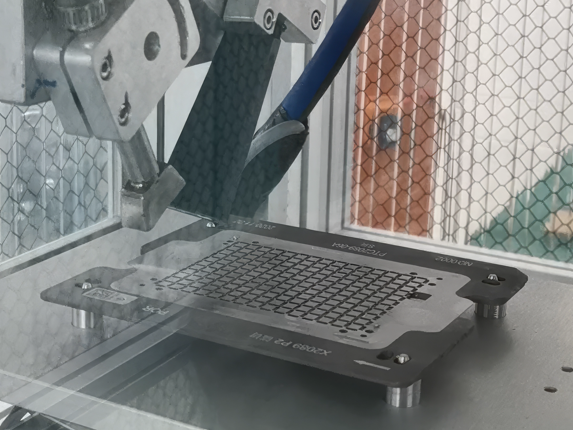
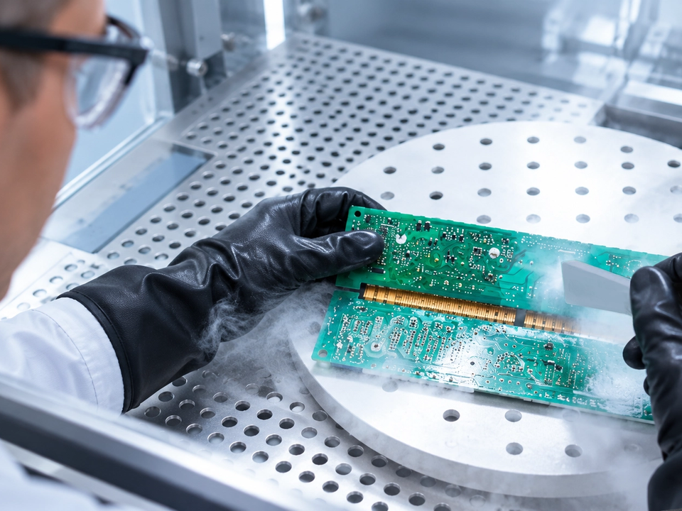
Dry ice blasting is a non-conductive, residue-free method for high-purity cleaning.
Solder Flux & Contaminant Removal
During PCB manufacturing, solder flux residue, solder balls, and cold soldered leads can remain on PCBs after welding and soldering processes, causing short circuits and component failures. Dry ice blasting provides a safe and effective way to remove these contaminants. Unlike traditional methods that use solvents or abrasive brushes, dry ice blasting is non-conductive and leaves no residue, ensuring the integrity of the board and its components without creating secondary waste. This makes it an ideal solution for cleaning PCBs, pogo pins, and in-circuit test (ICT) fixtures.
Surface Preparation & Coating Removal
Dry ice blasting effectively removes dust, flux residues, oils, and moisture contamination prior to conformal coating application. This non-abrasive cleaning method also excels at selective conformal coating removal during rework and repair operations, providing circuit board fabricators with a versatile solution that maintains component integrity while ensuring optimal surface conditions for subsequent processing steps.
General Maintenance & Component Cleaning
Dry ice blasting is highly effective for general maintenance of production equipment. It is an ideal solution for removing conformal coatings from spray coating fixtures. The process can also be used to remove surface rust from electrical harnesses and connectors, as well as to clean ceramic support discs and vacuum housing components. This allows technicians to clean sensitive equipment in-place without the risk of water damage or chemical contamination. The speed and efficiency of dry ice blasting reduce maintenance downtime, ensuring that critical production equipment remains operational and clean.
What Do Semiconductor Manufacturers Need for Dry Ice Cleaning?
Implementing dry ice blasting technology in your semiconductor manufacturing facility requires several key components:
Step 01
Dry Ice Cleaning Machine
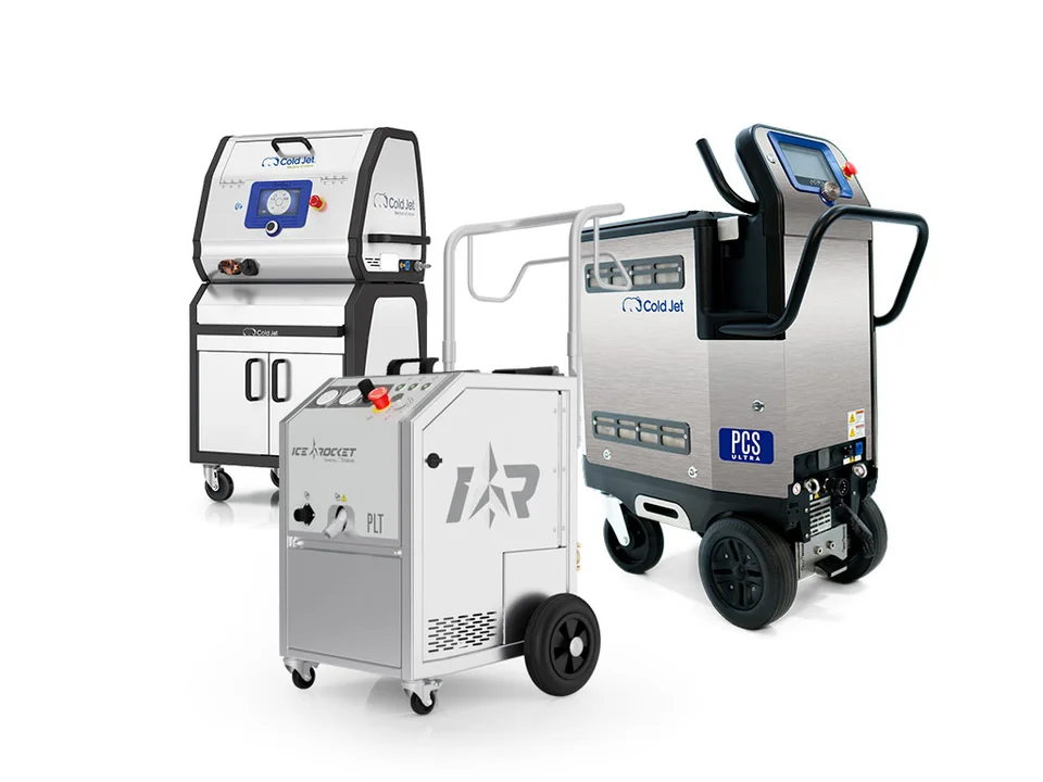
The foundation of any semiconductor cleaning process is a dry ice cleaning system designed for the industry’s stringent requirements. Cold Jet offers advanced dry ice blasters equipped with IoT connectivity and our proprietary Particle Control System (PCS®). This cutting-edge technology enables precise adjustment of cleaning parameters and particle dimensions, supporting both gentle surface preparation and intensive contamination removal. Each system includes specialized blast and air hoses, an applicator, and application-specific nozzles.
- 01. Dry Ice Cleaning Machine — The foundation of any semiconductor cleaning process is a dry ice cleaning system designed for the industry’s stringent requirements. Cold Jet offers advanced dry ice blasters equipped with IoT connectivity and our proprietary Particle Control System (PCS®). This cutting-edge technology enables precise adjustment of cleaning parameters and particle dimensions, supporting both gentle surface preparation and intensive contamination removal. Each system includes specialized blast and air hoses, an applicator, and application-specific nozzles.
- 02. Compressed Air — Semiconductor facilities can leverage their existing filtered compressed air networks. Cold Jet’s dry ice semiconductor cleaning machine typically operates at 100 cfm (2.8 m³/min) at 80 psi (5.5 bar), making integration easy.
- 03. Dry Ice Supply — Access to high-quality dry ice ensures continuous cleaning operations with your dry ice semiconductor cleaning equipment. Typical usage averages around 88 pounds per hour, though consumption varies depending on specific semiconductor applications and contamination levels. Our team can connect you with qualified dry ice suppliers and help establish delivery schedules that synchronize with your fabrication cycles.
- 04. Machine and Operator Training — Effective implementation requires thorough operator training on dry ice blasting techniques specific to semiconductor environments. Cold Jet provides specialized training that covers proper operating procedures and comprehensive safety practices tailored to cleanroom and semiconductor manufacturing environments.
- 05. Personal Protective Equipment (PPE) — When operating your dry ice semiconductor cleaning machine, cleaning personnel must utilize appropriate protective equipment, including gloves, hearing protection, and safety eyewear.
- 06. Automated Cleaning System (Optional) — Many semiconductor dry ice cleaning applications involve automated integration into existing production workflows. Complete automated solutions incorporate dry ice production equipment, one or multiple dry ice blasters, and robotic handling for seamless operation within semiconductor manufacturing lines.
How Dry Ice Blasting Compares to Alternatives
See how dry ice blasting stacks up against traditional cleaning methods across the criteria that matter most in semiconductor and PCB manufacturing.
| Criteria | Dry Ice Blasting Best | Chemical Cleaning | Manual Cleaning | Laser Cleaning |
|---|---|---|---|---|
| Secondary Waste | None – sublimates to gas, no residue | High – spent solvents and wastewater | Moderate – solvents, wipes, debris | Low – vaporized residue needs extraction |
| Speed | Fast – in-place, no disassembly | Slow – soak, rinse, dry cycles | Slow – hand wiping and scrubbing | Slow – point-by-point on surfaces |
| Equipment Damage | None – non-abrasive, no substrate damage | Possible – residue and corrosion | Possible – scratches delicate surfaces | Possible – heat can damage substrates |
| Regulatory Compliance | Strong – chemical-free, no waste | Limited – solvent and disposal rules | Inconsistent – operator dependent | Limited – VOC exposure |
| Downtime | Minimal – clean in-place, no cool-down | High – soak and dry time | High – disassembly and scrubbing | Moderate – slow per-surface setup |
| Environmental Impact | Low – no chemicals, reclaimed CO₂ | High – hazardous chemical disposal | Moderate – solvent and wipe waste | Moderate – generates VOC & energy intensive |
What Is the Best Dry Ice Blasting Machine for the Semiconductor Industry?
Cold Jet provides an extensive portfolio of dry ice semiconductor cleaning machines. Our intuitive, durable, and portable machines are ideal for cleanroom operations and semiconductor manufacturing facilities.
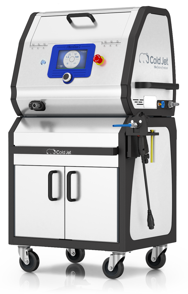
i3 MicroClean® 2
The i3 MicroClean 2 delivers cutting-edge precision cleaning technology optimized for semiconductor applications. This advanced dry ice blasting machine combines user-friendly operation with a compact, lightweight architecture. Ideal blasting parameters can be precisely locked in for each application. The i3 MicroClean 2 can be integrated as an automated solution.
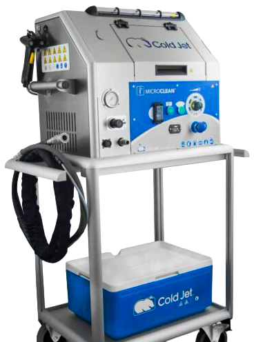
i3 MicroClean®
The i3 MicroClean offers exceptional efficiency in a streamlined package, demonstrating outstanding performance across diverse contamination removal and cleaning applications in semiconductor environments. The i3 MicroClean is capable of being integrated into a cleaning process as an automated solution.
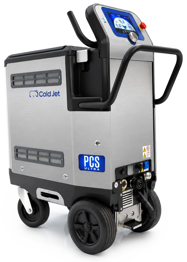
Aero2® PCS® ULTRA
The Aero2 PCS ULTRA delivers exceptional versatility for cleaning applications in the semiconductor industry. This advanced system is effective for gentle and precise surface cleaning using MicroParticle dry ice technology, as well as intensive cleaning of larger equipment surfaces utilizing 3mm dry ice pellets. The Aero2 PCS ULTRA is integration-ready and can be implemented in your process as an automated cleaning solution.
Which Dry Ice Blaster Fits Your Semiconductor Operation?
Compare the Cold Jet blasters suited to precision cleaning, so you can match particle control and cleaning intensity to process chamber components, wafer handling equipment, and tooling.
| Specification | i3 MicroClean® 2 | i3 MicroClean® | Aero2® PCS® ULTRA |
|---|---|---|---|
| Particle Control | Microparticles(Shaved) | Microparticles(Shaved) | Variable(0.3mm to 3.0mm, 28 sizes) |
| Controls | Digital(7" LCD, Recipes, IoT) | Analog / Standard | Digital(7" LCD, Recipes, IoT) |
| Feeder Technology | Radial Feeder | Radial Feeder | Two-Stage + Defrost Cycle |
| Application Intensity | Delicate / Precision | Delicate / Precision | Versatile(Precision to Aggressive) |
| Automation & Integration Capable | Yes | No | Yes |
| Hopper Capacity | 25 lbs(11 kg) | 20 lbs(9 kg) | 60 lbs(27 kg) |
Why Invest in Cold Jet Machines in the Semiconductor Manufacturing Industry?
When upgrading your cleaning technology in semiconductor device manufacturing, implementing Cold Jet dry ice cleaning technology is a strategic investment that enhances your operational performance. As you assess this capital investment, it’s essential to evaluate both the return on investment and the substantial competitive advantages dry ice blasting offers. Cold Jet systems consistently demonstrate accelerated payback periods and superior long-term value compared to alternative cleaning technologies.
Semiconductor and PCB manufacturers choose dry ice blasting for precision, residue-free cleaning. The non-abrasive, dry process removes contaminants in-place without chemicals, moisture, or secondary waste—protecting sensitive substrates while improving yield.
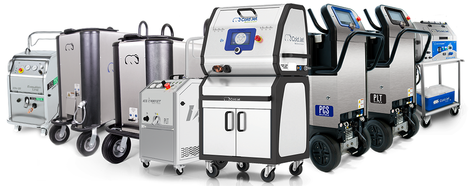
Semiconductor Cleaning Expertise
Cold Jet has developed unparalleled expertise in addressing the complex cleaning challenges and exacting standards that define semiconductor manufacturing environments.
Trusted by Semiconductor Manufacturers
With over 24,000 systems deployed worldwide, including installations at premier semiconductor fabrication facilities, Cold Jet has established itself as the preferred partner for critical cleaning applications in chip manufacturing and wafer processing operations.
Industry Leading Reliability
Our dry ice semiconductor cleaning equipment is specifically designed to withstand the rigorous demands of semiconductor production environments. Cold Jet dry ice cleaning systems deliver superior reliability and extended operational lifespans compared to competitors, ensuring minimal downtime.
Lower Operating Costs
Cold Jet systems are engineered for maximum efficiency, utilizing substantially less dry ice, compressed air, and electricity than competing dry ice blasting machines. This leads to reductions in your ongoing operational expenses.
Unmatched Support and Service
Our field service technicians provide immediate technical assistance when needed. We deliver preventive maintenance programs and thorough operator training to maximize your team’s effectiveness and system performance.
Application Specific Accessories
Our comprehensive catalog of specialized components, including precision applicators, blast hoses, and process-specific nozzles, enables you to configure the ideal cleaning solution for your unique semiconductor cleaning application.
Semiconductor manufacturers around the world rely on Cold Jet
Across a worldwide network of more than 24,000 installations, Cold Jet solutions range from hand-held dry ice blast cleaning machines to fully automated robotic solutions used for decontaminating equipment across the semiconductor manufacturing value chain.




Supporting Purity, Safety & Sustainability
Dry ice blasting helps semiconductor and PCB manufacturers meet contamination-control, worker-safety, and environmental goals without chemicals or secondary waste.
Contamination Control & Yield
Chemical residues, moisture, and particles left by conventional cleaning cause cross-contamination and downstream defects that lower yield.
Dry ice sublimates on contact, leaving zero residue, moisture, or secondary waste—preventing cross-contamination and preserving the purity essential for high yield.
Hazardous Chemical Exposure
Manual cleaning with harsh chemical solvents and high-pressure water exposes workers to hazardous substances and unsafe conditions.
Dry ice is non-toxic and eliminates harsh chemical solvents, improving occupational safety and removing worker exposure to hazardous chemicals.
Hazardous Waste Reduction
Solvent and chemical cleaning generate hazardous waste streams that require careful, costly disposal.
Dry ice blasting generates no secondary waste and uses no chemicals, reducing environmental impact and disposal costs with reclaimed CO₂.